Board · auxiliary supply
KA3843 / KA3845 Welder Auxiliary Power Boards
Identify the board by function, document every connector and test the startup, controller, switching and secondary sections in order. Board layout and rail values vary, so the reference ground is part of every measurement.
Identify the auxiliary-power board before applying a pin map
These boards are usually recognized by a small flyback transformer, one primary switching MOSFET, a KA3843/KA3845/UC3843/UC3845 controller, one or more secondary rectifiers, an optocoupler across the isolation slot and connectors leading to the control or driver board. Some machines integrate this stage into the main power board, so the physical board name is less important than the functional boundaries.
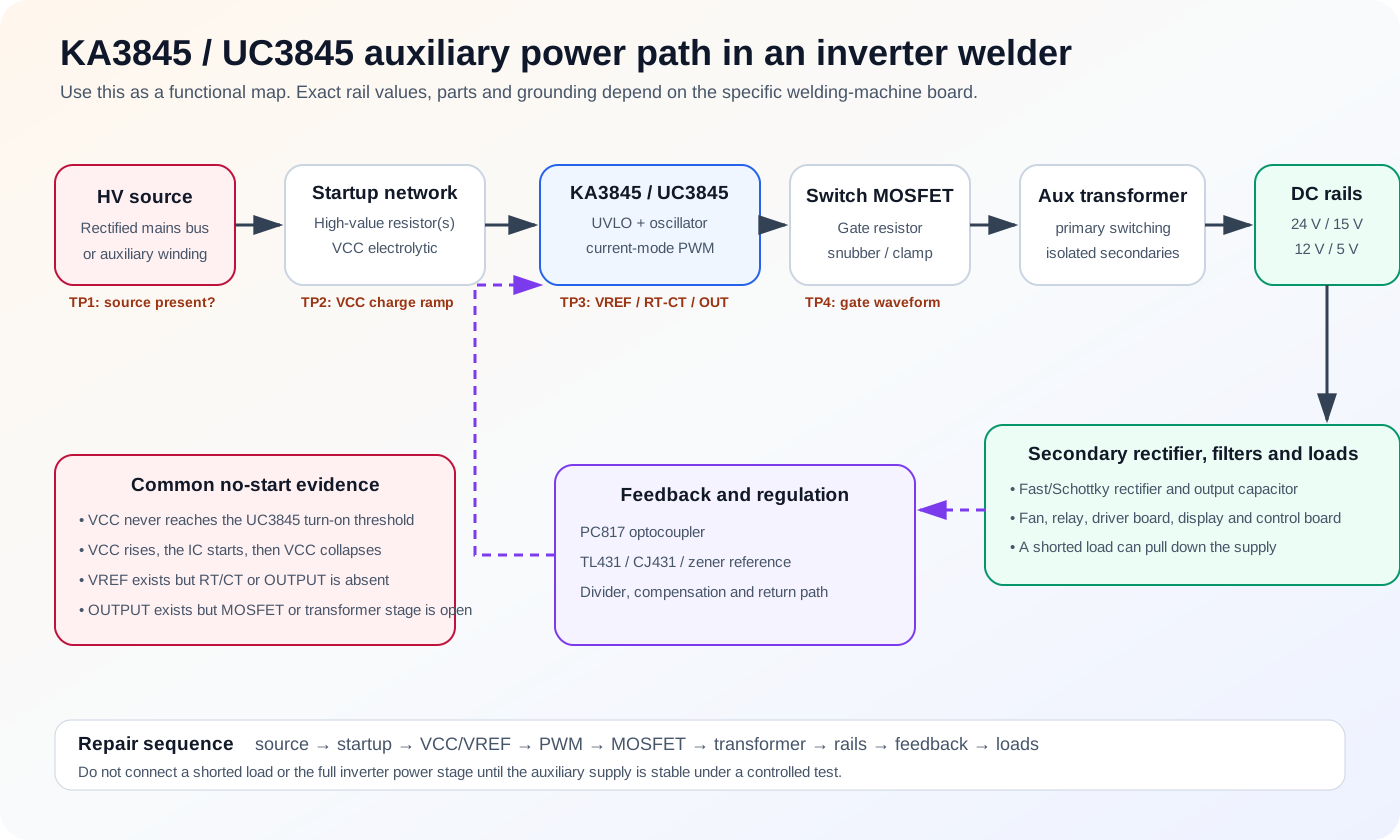
Connector inventory
| Connector group | Possible signals | Check before disconnecting |
|---|---|---|
| High-voltage/source input | Rectified bus or auxiliary AC feed | Discharge state, polarity, creepage and fuse/inrush path. |
| 24 V load output | Fan, relay, gas valve, wire feed or board distribution | Label return conductor and check load resistance. |
| Analog/driver output | ±15 V, 15 V or board-specific driver supply | Confirm whether rails are isolated or share a return. |
| Logic/display output | 5 V or regulated low-voltage feed | Check regulator location and connector polarity. |
| Enable/feedback | Remote enable, shutdown or sense return | Do not treat every thin wire as a power output. |
Power-rail map
Record every rail by connector pin, reference return, unloaded voltage and loaded voltage. A 24 V label on one welder may feed only a fan; on another it may power the relay, control board and driver chain. Never infer the whole board state from one connector pin.
Minimum useful test-point record
| Point | Reference ground | Evidence to record |
|---|---|---|
| Bus input to startup network | Primary bus negative | Source present and stable. |
| Controller VCC | Controller ground pin | Ramp, peak, minimum and cycle period. |
| Controller VREF | Controller ground pin | Stable reference and response to external-load isolation. |
| RT/CT | Controller ground pin | Oscillator waveform. |
| OUTPUT / MOSFET gate | Controller/MOSFET source reference | Pulse presence, amplitude and edge quality. |
| Each secondary output | Matching secondary return | Voltage, ripple and load response. |
KA3843 / KA3845 controller section
Confirm the package and manufacturer before using a pin table. On the common 8-pin layout, trace COMP/VFB feedback, ISENSE, RT/CT, ground, output, VCC and VREF. A controller replacement is justified only after the startup feed, timing network, current-sense path, gate load and VREF loads have been checked.
Common board faults
- Open startup resistor chain or heat-cracked solder joint.
- High-ESR VCC capacitor that cannot support the first switching pulses.
- Shorted switching MOSFET, damaged gate resistor or source-current resistor.
- Shorted secondary rectifier or filter capacitor.
- Open optocoupler LED path or unstable TL431 compensation.
- Connector corrosion, reversed repair wiring or shorted external load.
- Carbonized isolation slot or contamination causing leakage.
Safe probing rules
- Photograph and label connectors before removal.
- Mark primary and secondary returns on the board image.
- Use rated probes and an isolation-safe scope method.
- Measure one node at a time; do not move a ground clip on a live primary.
- Keep the full inverter power stage disconnected until auxiliary rails and gate behavior are stable.
- Reconnect loads individually and monitor rail collapse or heating.
Stop conditions before another power-up
- Connector pinout or polarity is not documented.
- Primary and secondary returns cannot be distinguished.
- A MOSFET, rectifier or output rail remains shorted.
- Isolation spacing is carbonized or damaged.
- Gate drive is missing or unstable with the switching device connected.
- A downstream load immediately pulls a rail down or overheats.
Technical sources
- Texas Instruments UC3845 product page — pin functions, UVLO, VREF, current limit and maximum duty-cycle reference.
- UCx84x current-mode PWM controller datasheet — controller-level limits; it does not replace the actual board schematic.
- Texas Instruments TL431 product page — secondary feedback reference when the board uses TL431/KA431 regulation.
- WelderData internal technical records — used for measurement sequence and repair-pattern organization; exact readings remain board-specific.
Related repair map
Follow the evidence path from symptom to measurement, circuit and repair case.