Auxiliary power PWM repair reference
KA3845 / UC3845 Welder Auxiliary Power Pinout and No-Start Diagnosis
Use this page when an inverter welder is dead, has no 24 V control rail, makes a repeated ticking sound, starts and immediately collapses, or uses a KA3845 / UC3845-style eight-pin controller in the auxiliary switching supply.
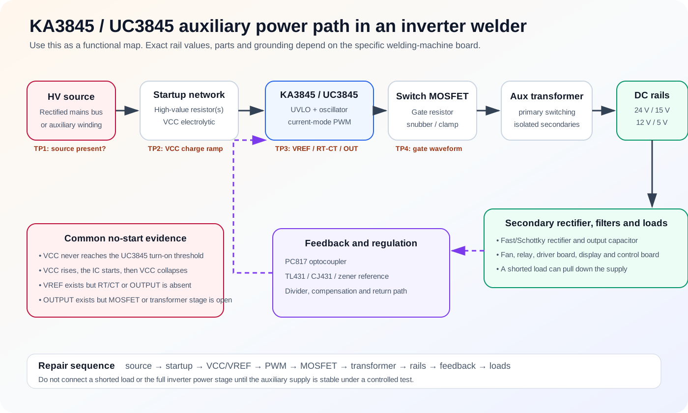
Quick repair map
What to measure first
Scope: 8.4 V / 7.6 V UVLO, nominal 5 V VREF, the 1 V current-sense limit and 50% maximum duty cycle are UC3845 device-level references. A real welder's steady VCC, switching frequency, transformer ratio and secondary rail values are board-specific and are not a universal welder reading.
What KA3845 / UC3845 does in an inverter welder
The UC3845 belongs to the UCx84x current-mode PWM-controller family. In an auxiliary supply it combines an undervoltage lockout, a fixed-frequency oscillator, an error amplifier, pulse-by-pulse current limiting and a totem-pole output intended to drive an N-channel MOSFET. The UC3845 variant limits maximum duty cycle to 50%, which is useful in many transformer-coupled flyback or forward-style auxiliary supplies.
On a welding-machine board, this small supply is often responsible for the rails that wake the rest of the machine: 24 V for a fan or relay, 15 V for gate-driver or analog circuits, 12 V for control functions and 5 V for logic or display electronics. A failure in this stage can therefore make the entire welder look dead even when the main rectified DC bus is present.
A board marked KA3845 often follows the same eight-pin current-mode-control pattern, but manufacturer details and electrical limits must be checked before substitution. Treat the shared “3845” number as a diagnostic clue, not automatic proof that every branded part is a drop-in replacement.
Package appearance, marking and pin-one orientation
The most common repair target is an 8-pin PDIP or SOIC package. TI also documents a 14-pin SOIC option in the wider UCx84x family, so never assume the pin numbering from the visible “3845” text alone. Confirm the package, the notch or dot and the manufacturer's exact data before probing.
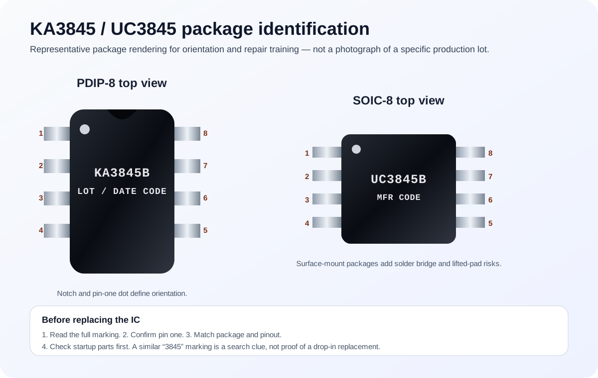
Do not judge authenticity or compatibility from typography alone. Production markings vary by manufacturer, lot and package. A useful photo for repair must show the complete top marking, pin-one indicator and enough board context to establish orientation; random product-listing images often fail those tests.
Real-world visual identification reference
Use this reconstructed visual to recognize the general package shape, pin-one orientation and the kind of board area where the device is commonly found. It is a visual identification aid, not proof that a particular welder uses the same package, marking or surrounding components.
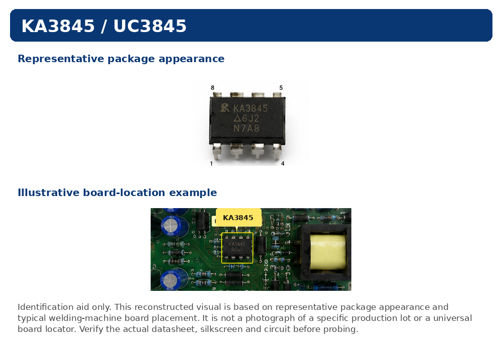
Before probing, confirm the actual device marking, package, board silkscreen and manufacturer datasheet. The board-location panel is illustrative and must not be treated as a universal component locator.
KA3845 / UC3845 8-pin repair table
| Pin | Name | Device function | First welder-board check |
|---|---|---|---|
| 1 | COMP | Error-amplifier compensation and PWM command node. | Check whether feedback, a protection transistor or a failed compensation capacitor clamps COMP low. Forcing COMP to ground commands zero duty cycle. |
| 2 | VFB | Inverting input of the internal error amplifier; nominal regulation point is around 2.5 V. | Trace the PC817/TL431 or zener feedback divider. An open optocoupler path, drifted divider or bad solder joint can drive output high, low or into pulsing restart. |
| 3 | ISENSE | Primary current-sense input used to terminate each pulse; device-level maximum signal is typically about 1 V. | Inspect the source resistor, current-transformer path, RC filter and noise spikes. A false current pulse can shut down every switching cycle. |
| 4 | RT/CT | Oscillator timing node. The resistor connects toward VREF and the timing capacitor toward ground. | Look for the oscillator waveform with an isolated oscilloscope setup. Check a cracked timing capacitor, drifted resistor, contamination and damaged trace. |
| 5 | GROUND | Analog and power ground on the common 8-pin package. | Use this reference for VCC, VREF and low-side signal measurements. Verify that the board's primary-side ground is not confused with secondary or chassis ground. |
| 6 | OUTPUT | Totem-pole gate-drive output, actively held low while VCC is below turn-on. | Check pulse amplitude, duty and edge quality. If present, continue to the series gate resistor, buffer transistor if fitted, MOSFET gate and transformer primary. |
| 7 | VCC | Controller bias input. TI recommends 12 V to 28 V for operation; UC3845 UVLO typically turns on near 8.4 V and off near 7.6 V. | Watch the startup ramp. If VCC never reaches turn-on, inspect the startup resistor and leakage. If it rises then collapses, inspect sustaining power, the VCC capacitor and secondary loading. |
| 8 | VREF | Nominal 5 V reference for the timing and control circuitry. | Measure after VCC has crossed UVLO. If low, isolate the bypass capacitor and external loads. Do not replace the IC until an overloaded reference rail is excluded. |
Pin functions above follow the common 8-pin UC3845 arrangement. If the actual board uses a 14-pin package or another manufacturer variant, use that exact datasheet before applying these locations.
Safe measurement order for a dead or ticking auxiliary supply
- Record the symptom before power is applied. Note whether the fan twitches, relay chatters, display flashes, VCC pulses or the series lamp repeatedly brightens and dims.
- Perform unpowered resistance checks. Discharge the bus, then check the switching MOSFET, primary current-sense resistor, secondary rectifiers and rail-to-ground resistance. A hard short must be resolved before live testing.
- Confirm the source feeding the startup resistor. The source may be the main HV DC bus or a separate auxiliary winding. Missing source voltage points upstream, not to the KA3845 / UC3845.
- Observe pin 7 VCC as a waveform, not only a single number. A healthy startup should cross the turn-on threshold and then remain above the turn-off threshold. A sawtooth rise-and-collapse pattern is strong evidence of a sustaining or load fault.
- Check pin 8 VREF. A stable nominal 5 V reference proves more than VCC alone. If VREF is low, disconnect external reference loads or the bypass capacitor as appropriate before deciding that the IC is damaged.
- Check RT/CT and OUTPUT. Timing activity at pin 4 should lead to switching at pin 6 unless COMP, VFB, ISENSE or an external circuit is blocking operation.
- Follow the energy path downstream. With PWM present, inspect the gate resistor, MOSFET, snubber/clamp, transformer primary, secondary rectifier and filter capacitors.
- Reconnect loads one group at a time. Fan, relay, driver board, display and logic rails should be reintroduced only after the unloaded supply is stable under current limiting.
No-start decision tree
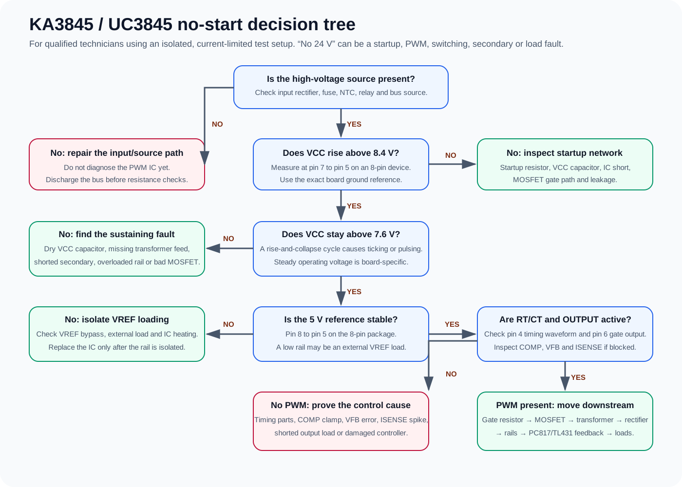
How to interpret common VCC patterns
| Observed evidence | Likely meaning | Next proof |
|---|---|---|
| VCC remains near zero | No startup feed, open startup resistor, shorted VCC rail or severe IC/MOSFET leakage. | Power off, verify source and resistance from VCC to ground, then check the high-value startup chain. |
| VCC climbs but never reaches 8.4 V | Startup current is insufficient or leakage is too high. | Measure resistor values out of circuit when necessary; inspect the small electrolytic and any zener clamp. |
| VCC crosses 8.4 V then falls below 7.6 V repeatedly | The IC starts but the supply cannot sustain itself. This often causes ticking, relay chatter or a flashing display. | Check auxiliary winding feed, VCC diode/capacitor, shorted secondary rectifier, overloaded rail and switching MOSFET behavior. |
| VCC and VREF stable, no RT/CT waveform | Timing network fault, damaged oscillator, contamination or a connection error. | Check pin 4 parts and ground return. Confirm the exact package and pin orientation. |
| RT/CT active, no OUTPUT | COMP is clamped, VFB commands minimum duty, ISENSE is falsely high, output pin is loaded or the IC is damaged. | Compare pins 1–3, isolate the output load and inspect the feedback/protection transistor path. |
| OUTPUT present, no secondary rails | Fault is downstream of the PWM controller. | Check gate waveform at the MOSFET, MOSFET switching, transformer continuity, secondary rectifier and filter. |
| Rails recover when a connector is unplugged | The auxiliary supply may be healthy; the disconnected fan, relay, driver or control board is pulling it down. | Measure each load separately and reconnect through current limiting. |
Common peripheral failures before the IC
Startup resistor chain
High-value resistors can go open or drift upward. A meter reading in circuit can be misleading if parallel paths exist.
Small VCC electrolytic
Loss of capacitance or high ESR produces unstable startup, ticking and short bursts of output even when the IC is good.
Switching MOSFET and gate path
A shorted MOSFET, leaky gate, open series resistor or damaged clamp can prevent the supply from starting or destroy the replacement controller.
Current-sense path
An open sense resistor, bad filter or noise spike at ISENSE can terminate each pulse and imitate a controller fault.
Secondary rectifier and capacitors
A shorted diode or electrolytic on the 24 V / 15 V rail can force repeated UVLO restart.
PC817 and reference network
An optocoupler, TL431/CJ431, zener or divider fault can command the wrong duty cycle or destabilize regulation.
Stop conditions before reconnecting the full machine
- Do not reconnect the full load while a secondary rail measures as a hard short.
- Stop if the switching MOSFET is shorted, the gate resistor is open or the snubber/clamp is visibly burnt.
- Stop if VCC repeatedly crosses UVLO and collapses without a known, isolated cause.
- Stop if the OUTPUT waveform is continuously high, heavily distorted or referenced to the wrong ground.
- Stop if the main bus cannot be safely discharged and verified before resistance measurements.
- Do not connect the inverter IGBT/MOSFET power stage merely because the 24 V rail returned; first verify driver rails and gate-drive permission.
- Use isolation, current limiting and properly rated probes. Primary-side ground is live with respect to earth in many auxiliary supplies.
Frequently asked repair questions
Is 8.4 V a normal steady VCC reading?
No. It is the typical UC3845 turn-on threshold, not a universal steady operating value. TI's recommended operating supply range is 12 V to 28 V, but the actual stable VCC on a welder board depends on its auxiliary winding, clamp and load.
Why does the supply tick every second?
VCC may charge through the startup resistor, cross 8.4 V, start switching and then collapse below 7.6 V because sustaining power is missing or a secondary load is excessive. Watching VCC with an oscilloscope or recording min/max values is more useful than a single multimeter number.
Can I replace KA3845 with UC3845?
Only after confirming the exact manufacturer datasheets, pinout, package, UVLO thresholds, duty-cycle behavior, temperature grade and board circuit. Similar numbering does not by itself prove safe substitution.
VREF is 5 V, but there is no 24 V. Is the chip good?
A stable VREF proves that the bias and reference sections are alive, but it does not prove oscillator, output, MOSFET, transformer, rectifier, feedback or load health. Continue through RT/CT and OUTPUT.
Can I test the chip without the main inverter stage connected?
Often the auxiliary supply can be evaluated with downstream loads isolated, but the exact method depends on board topology. Preserve any required feedback load, use current limiting and never assume that removing a connector makes the primary side safe.
Technical sources and scope
The UC3845 pin functions, 8.4 V turn-on and 7.6 V turn-off thresholds, nominal 5 V reference, 50% maximum duty cycle, current-sense behavior and package options are checked against the official Texas Instruments UC3845 product page and the UCx84x current-mode PWM controller datasheet.
WelderData does not copy an unlicensed marketplace or forum photograph into this article. The package image and functional diagrams are original technical illustrations derived from official pin data and the project's welding-machine repair material. They identify orientation and repair nodes but do not claim to represent a particular manufacturer's lot or a specific welder board.
Exact VCC, frequency, transformer pinout, feedback polarity, rail voltage and load arrangement remain board-specific. Use the actual schematic, board labels and a known-good comparison whenever available.
Last technical review: July 13, 2026.
Related repair map
Follow the evidence path from symptom to measurement, circuit and repair case.