Chip reference
HCPL-316J IGBT Gate Driver Reference for Welder Power Boards
A WelderData reference for dedicated optically isolated IGBT gate-driver circuits, UVLO, desaturation protection, fault feedback and push-pull gate-output checks on welding-machine power boards.
Database summary
The HCPL-316J is an optically isolated IGBT gate-driver device used in power-electronics boards where the controller side must be isolated from the high-energy switching stage. In welder repair, this family of driver is useful to understand because it combines drive isolation, gate output, undervoltage lockout, desaturation / overcurrent detection and fault feedback in one driver architecture.
WelderData treats this page as a repair reference, not as a claim that every inverter welder uses HCPL-316J. Many ZX7-style machines use gate-drive transformers or discrete driver stages. The diagnostic principles overlap: verify the gate-drive supply, turn-on bias, turn-off bias, gate resistor path, discharge path, protection feedback and fault-clear logic before installing a replacement IGBT.
WelderData circuit map
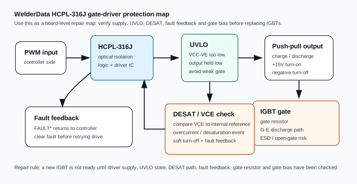
The map separates the controller-side PWM input from the isolated driver side. A repair check should not stop at the PWM input: weak driver supply, UVLO, DESAT, a stuck fault line, a failed push-pull transistor or an open gate resistor can all prevent a correct gate waveform.
Gate-drive bias requirements
| Item | Repair reference | Why it matters |
|---|---|---|
| Positive gate bias | Commonly +12V to +15V | Too low can leave the IGBT in a high-loss region instead of firm saturation. |
| Negative turn-off bias | Often -2V to -10V depending on design | Improves turn-off immunity and helps prevent false triggering from dv/dt noise. |
| Gate resistor | Usually several ohms to tens of ohms | Too high slows switching and raises loss; too low increases current rise and noise stress. |
| Discharge path | Low-impedance G-E discharge path required | A floating gate or open discharge path can make a good IGBT fail after replacement. |
| Static handling | Do not leave G-E open without protection | The IGBT gate is capacitive and vulnerable to stored charge and static events. |
UVLO: weak driver supply protection
Undervoltage lockout prevents the driver from applying a weak gate signal when the isolated driver supply is below its usable range. In the HCPL-316J architecture, output is held low when the VCC-to-VE supply is below the UVLO threshold, commonly referenced around 12V in service notes.
For repair work, UVLO means that a missing gate waveform does not automatically prove the PWM controller is dead. Confirm the isolated driver supply first. If the driver supply never reaches the required range, the output may remain low by protection design.
DESAT / overcurrent protection
Desaturation protection monitors the IGBT collector-emitter voltage during conduction. When VCE remains too high while the gate is commanded on, the driver interprets the event as desaturation or overcurrent and shuts the IGBT down while returning a fault signal to the controller side.
A common service reference for this driver family is an internal comparison level around 7V. In practice, external diode drops and blanking components affect the actual trip behavior. Do not bypass this path during repair. A failed DESAT diode, open blanking capacitor, shorted sense path or uncleared fault line can make the driver appear dead or can allow repeated IGBT destruction.
Push-pull output stage checks
The HCPL-316J output is often followed by a transistor push-pull stage to increase gate charge and discharge current. When the driver output is high, the upper device charges the IGBT gate toward the positive bias rail. When the output is low, the lower device pulls the gate toward the negative turn-off rail or discharge reference.
- Measure the positive and negative driver rails before judging the gate pulse.
- Check the gate resistor and the G-E discharge path for open, drifted or cracked parts.
- Check the push-pull transistors for shorts that clamp the gate high or low.
- Verify that the fault feedback has been cleared before expecting a new output pulse.
Symptoms and repair routing
| Observed condition | Likely driver-side route | Next check |
|---|---|---|
| PWM input present but no gate output | UVLO, fault latch, failed driver supply or damaged output stage | Check VCC-VE, fault line, clear input and push-pull transistors. |
| Gate output weak or slow | Low driver supply, wrong gate resistor, overloaded driver or damaged transistor | Compare turn-on and turn-off bias with the board design. |
| IGBT fails immediately after replacement | DESAT disabled, gate resistor open, no negative bias, missing discharge path or fault feedback ignored | Do not energize again until the driver protection path is verified. |
| Driver trips under load | Real overcurrent, DESAT sense fault, wrong blanking behavior or bad IGBT module | Separate load fault from detection-circuit fault using controlled power-up. |
Dedicated driver module comparison
HCPL-316J-style optically isolated drivers and M57962AL-style driver modules are different implementations, but a welder repair path treats both as protected IGBT drive systems. Before replacing another power module, verify driver supply, gate output, protection feedback, short-circuit evidence and soft-shutdown or fault-latch behavior.
| Item | HCPL-316J-style driver | M57962AL-style module |
|---|---|---|
| Isolation and gate drive | Optically isolated driver with external gate network | Dedicated IGBT driver module with gate output and protection functions |
| Protection evidence | UVLO, DESAT and fault feedback | Short-circuit detection, fault output and soft shutdown behavior |
| WelderData rule | No new IGBT should be fitted until the driver supply, gate resistor, clamp network, fault line and load-side short evidence are recorded. | |