Fails immediately at power-up
Prioritize an unresolved power-stage short, cross-conduction, reversed device, gate held on, missing dead time or incorrect bridge wiring.
Fault · repeated power-device failure
Repeated IGBT failure is rarely solved by replacing only the shorted devices. Isolate the power stage, controller, protection, driver and each gate branch before restoring DC-bus energy.
Prioritize an unresolved power-stage short, cross-conduction, reversed device, gate held on, missing dead time or incorrect bridge wiring.
Prioritize current feedback, overcurrent protection, output rectifier, transformer or load-side faults that appear under current.
Compare only that gate branch against a known-good branch: resistor, transformer secondary, clamp, connector, solder and thermal contact.
Investigate controller timing, complementary drive, bus overshoot, snubber/clamp failure and full-bridge commutation.
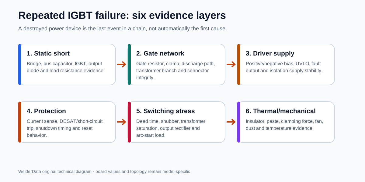
Six-layer sequence: Static short → Gate network → Driver supply → Protection → Switching stress → Thermal/mechanical.
| Layer | Reference | Evidence | Do not continue when |
|---|---|---|---|
| DC bus | Bus positive to bus negative | Short resistance trend, bridge and capacitor condition | Low resistance remains unexplained. |
| Power devices | Each device terminals | Same-polarity diode-mode and resistance comparison | One device or antiparallel diode differs materially. |
| Gate network | Gate to emitter/source | Gate resistor, discharge resistor, clamp and trace continuity | A gate is open, shorted or connected to the wrong emitter return. |
| Driver isolation | Primary and each isolated secondary | Winding resistance and insulation boundaries | A winding is open or isolation is carbonized. |
| Snubber/clamp | Across the intended switching node | Capacitor, resistor, diode and MOV condition | Energy-clamp parts are open, shorted or heat damaged. |
| Output stage | Secondary rectifier/output return | Rectifier, choke, cable and output short | The load-side short has not been isolated. |
Use the controller ground for UC3846 or SG3525 measurements, the driver-module return for a hybrid driver, and each device emitter/source for the final gate waveform. These nodes may not be interchangeable.
Absolute gate voltage, negative bias, pulse width and dead time depend on the actual board. The reliable repair method is to compare equivalent branches under the same low-energy condition.
| Compare | Reference ground | Abnormal evidence | Likely area |
|---|---|---|---|
| Controller output A vs B | Controller ground | One output absent or distorted | Controller, shutdown logic or output loading. |
| Driver primary channels | Primary driver return | Different amplitude or timing | Buffer transistor, coupling network or transformer primary. |
| Transformer secondary channels | Matching secondary return | One winding weak, inverted or absent | Transformer winding, rectifier/clamp or connector. |
| Gate-emitter waveforms | That device emitter | Slow turn-off, false pulse or missing negative bias | Gate resistor, clamp, emitter lead or driver supply. |
Resolve VCC, VREF, oscillator, shutdown, current sense and feedback first.
Check buffer transistors, coupling capacitors/resistors, dead-time network and driver-enable logic.
Check the driver transformer winding, secondary rectifier/clamp and connector path.
Check polarity, device matching, heatsink contact, bus overshoot, output short and current-protection response.
Check shunt/current transformer polarity, burden parts, current-sense filtering and actual output-stage current.
Check thermal interface, fan airflow, cracked solder, intermittent connector and gate resistance changing with heat.
Follow the evidence path from symptom to measurement, circuit and repair case.