Current-mode PWM repair reference
UC3846 Welder PWM Controller: Pin Checks and No-PWM Diagnosis
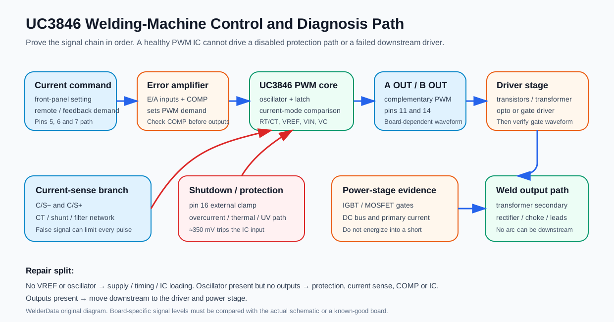
Measure in this order: VIN/VC → VREF → RT/CT → shutdown/current sense → A/B outputs → downstream driver.
Safe measurement order: fast diagnostic sequence
| Order | Measure | Expected evidence | If missing |
|---|---|---|---|
| 1 | Pin 15 VIN and pin 13 VC to pin 12 GND | Stable board-specific supplies; no repeated rise/collapse. | Repair auxiliary supply, connector, regulator or decoupling first. |
| 2 | Pin 2 VREF | Approximately 5.1 V. | Isolate VREF loads; check capacitor and IC. |
| 3 | Pins 8 CT and 9 RT | Stable timing ramp/oscillator activity. | Check CT, RT, sync, tracks and soldering. |
| 4 | Pin 16 Shutdown | Below the active trip level; typical threshold 350 mV. | Trace overcurrent, thermal, undervoltage and inhibit circuits. |
| 5 | Pins 3/4 and pin 7 COMP | No false current-limit signal or forced-low PWM command. | Check CT/shunt, filters, feedback and clamps. |
| 6 | Pins 11 and 14 | Complementary, comparable A/B pulses. | Check VC, output loading or IC output-stage damage. |
| 7 | Driver input to gate | Both branches remain symmetrical through the driver. | Check buffers, transformer/isolator, gate resistors and clamps. |
Measurement conditions
| Check | Required condition | Why it matters |
|---|---|---|
| DMM voltage checks | Measure against pin 12 local control ground, not chassis or power-emitter ground unless the schematic joins them. | A wrong reference can make healthy VIN, VREF, COMP or shutdown levels look incorrect. |
| Oscilloscope timing checks | Use an isolated/differential method appropriate to the board. Keep the probe ground away from the rectified mains domain. | A grounded bench scope can short a floating primary and destroy the board or instrument. |
| Control-only test | Where the board design permits, prove VREF, RT/CT, shutdown and A/B outputs with the power stage disconnected or on a low-energy current-limited supply. | This separates controller evidence from IGBT, transformer and output-stage faults. |
| Channel comparison | Compare pin 11 with pin 14, then compare both complete driver branches at the same test points. | Absolute waveform amplitude is board-dependent; branch symmetry is often the stronger repair clue. |
| Loaded versus unloaded output | If an output is missing, isolate its downstream buffer only when the circuit allows safe separation. | A shorted buffer can suppress a healthy IC output and lead to an incorrect controller replacement. |
Visual identification
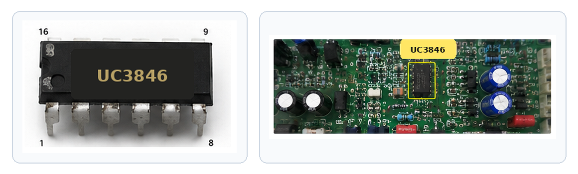
UC3846 is available in 16-pin PDIP; UC3846DW identifies the 16-pin SOIC package. Verify manufacturer and package before substitution.
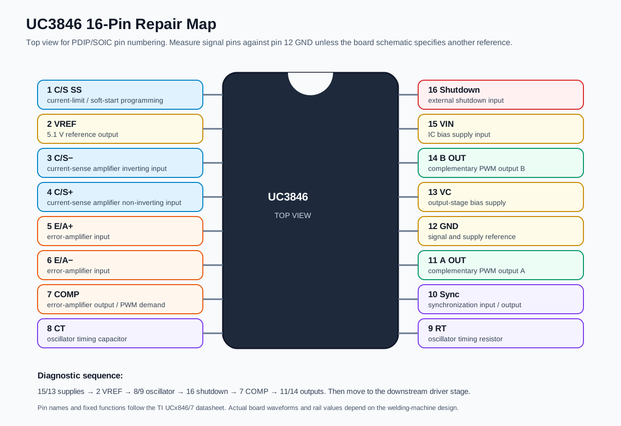
UC3846 16-pin repair map
| Pin | Name | Function | First repair check |
|---|---|---|---|
| 1 | C/S SS | Current-limit / soft-start programming | Check the RC network and any transistor that clamps startup. |
| 2 | VREF | 5.1 V reference output | Measure to pin 12. Isolate loads before replacing the IC. |
| 3 | C/S− | Current-sense amplifier inverting input | Compare with pin 4; inspect CT/shunt burden and filter parts. |
| 4 | C/S+ | Current-sense amplifier non-inverting input | Look for false DC offset or switching spikes. |
| 5 | E/A+ | Error-amplifier non-inverting input | Check command/reference input and divider network. |
| 6 | E/A− | Error-amplifier inverting input | Check feedback, optocoupler and current/voltage regulation path. |
| 7 | COMP | Error-amplifier output / PWM command | A low clamp can suppress both outputs. |
| 8 | CT | Oscillator timing capacitor | Confirm a clean ramp; check leakage and solder joints. |
| 9 | RT | Oscillator timing resistor | Check resistor value, trace continuity and contamination. |
| 10 | SYNC | Synchronization input/output | Check for an external clamp or noise that disrupts timing. |
| 11 | A OUT | Complementary PWM output A | Compare amplitude and timing with pin 14. |
| 12 | GND | Control reference | Verify continuity to local control ground before trusting readings. |
| 13 | VC | Output-stage supply | Logic can run while the output stage lacks VC. |
| 14 | B OUT | Complementary PWM output B | Compare with pin 11; unequal branches can damage the driver. |
| 15 | VIN | Controller bias supply | Check level, ripple and undervoltage cycling. |
| 16 | Shutdown | Fast shutdown input | Typical threshold is 350 mV; trace the protection source. |
Supply and reference checks
| Evidence | Likely fault area | Next action |
|---|---|---|
| No VIN at pin 15 | Auxiliary supply, connector, regulator or open feed | Repair supply before testing the controller. |
| VIN stable; VC missing at pin 13 | Output-stage feed or local decoupling | Trace VC feed; logic may run with no output drive. |
| VIN rises and collapses | UVLO cycling, overloaded supply or bad capacitor | Check ripple, startup path and downstream load. |
| VREF below 5 V | External load, shorted capacitor or IC damage | Isolate VREF consumers before replacing the IC. |
Device facts versus board values
| Item | Device-level reference | Board-level interpretation |
|---|---|---|
| VREF | Nominal 5.1 V; the official electrical range is approximately 5.00–5.20 V under specified conditions. | A loaded reference can read low even when the IC is not the root cause. |
| Shutdown | 250–400 mV threshold range, 350 mV typical. | Noise, leakage or a real protection signal can trip it; identify the source before forcing it low. |
| VIN and VC | Separate controller and output-stage supply pins. | The exact operating levels and ripple limit are board-dependent. Both must remain stable. |
| Oscillator and outputs | Current-mode controller with complementary A/B outputs. | Frequency, dead time, pulse width and output amplitude are selected by the welder design. |
Timing and control-loop checks
| Observation | Check | Interpretation |
|---|---|---|
| VREF present; no CT ramp | Pins 8/9, CT leakage, RT open, pin 10 sync loading | No valid timing means no valid A/B output. |
| Timing stable; COMP held low | Error-amplifier inputs, feedback optocoupler and clamps | The loop is commanding minimum duty or protection is overriding it. |
| Frequency unstable | CT, RT, VREF noise, ground and sync | Repair timing integrity before testing the power stage. |
| COMP active but output duty abnormal | Current-limit/soft-start network at pin 1 and current sense | Separate control command from pulse-by-pulse limiting. |
Shutdown and current-sense checks
| Node | Fault evidence | Trace next |
|---|---|---|
| Pin 16 above trip threshold | Both outputs suppressed or latched off | Protection comparator, optocoupler, transistor, thermal and undervoltage paths. |
| Pins 3/4 show unexplained differential signal | False pulse-by-pulse current limiting | Current transformer/shunt, burden resistor, rectifier and RC filter. |
| Pin 1 cannot ramp | Soft-start/current-limit network clamped | Capacitor leakage, transistor clamp or shorted trace. |
| Shutdown clears but immediately returns | Real downstream fault or noisy protection signal | Test with low energy; inspect driver/power stage before bypassing protection. |
A/B outputs and downstream driver
| Observation | Likely area | Action |
|---|---|---|
| Both outputs absent; prior checks valid | VC supply, output loading or IC output stage | Verify pin 13 and isolate downstream load where safe. |
| Only A or B missing | Damaged output, buffer transistor or open trace | Compare pins 11/14 directly at the IC. |
| A/B correct at IC; missing at driver transformer | Buffer/coupling network | Check transistors, resistors, capacitors and transformer primary. |
| Driver secondary or gates unequal | Transformer branch, clamp, gate resistor or device loading | Do not install power devices until both branches agree. |
| Gate drive correct; no welding output | Power switch, transformer, secondary rectifier or output path | Move beyond the PWM controller. |
No-PWM decision tree and workflow
- Confirm pin 12 is the correct local control ground.
- Confirm stable VIN at pin 15 and VC at pin 13.
- Confirm approximately 5.1 V at pin 2.
- Confirm RT/CT oscillator activity at pins 9/8.
- Confirm pin 16 is not being driven into shutdown.
- Check pin 1, pins 3/4 and pin 7 for current-limit or command suppression.
- Compare pins 11 and 14.
- If A/B outputs are correct, follow the buffer, transformer/isolator and gate network.
| Last confirmed good point | Fault zone |
|---|---|
| No VIN/VC | Auxiliary/control supply |
| VIN/VC present; no VREF | VREF load or UC3846 |
| VREF present; no timing | RT/CT/sync/oscillator |
| Timing present; shutdown active | Protection chain or real downstream fault |
| Control valid; no A/B | VC, output loading or IC output stage |
| A/B valid; no gate drive | Downstream driver |
Stop conditions before power-stage testing
- Do not connect the power stage until the driver stage has two valid, non-overlapping branches and the protection cause is understood.
- Do not energize with a shorted IGBT/MOSFET or shorted DC bus.
- Stop if A/B pulses are missing, overlapping, heavily distorted or unjustifiably unequal.
- Stop if driver-transformer branches, gate resistors or gate discharge paths do not match.
- Stop if shutdown remains active and the protection source is unknown.
- Stop if VIN/VC repeatedly rises and collapses.
- Use current-limited staged power-up only after control, driver and resistance checks agree.
Related repair map
Follow the evidence path from symptom to measurement, circuit and repair case.