PWM controller repair reference
SG3525A Welder PWM Controller: Pin Checks and No-PWM Diagnosis
Use the checks below to separate controller, timing, shutdown, output-supply and downstream driver faults.
Fast diagnostic sequence
| Order | Measure | Expected evidence | If missing |
|---|---|---|---|
| 1 | Pin 15 VCC to pin 12 GND | Stable controller supply within the board design and device operating range. | Repair the auxiliary supply, ground path or local decoupling first. |
| 2 | Pin 16 VREF | Approximately 5.1 V. | Check VCC, VREF loading and the IC. |
| 3 | Pin 5 CT and pin 4 oscillator output | Timing ramp and clock activity. | Check RT, CT, discharge, sync and timing traces. |
| 4 | Pin 8 soft-start | Rises after startup; not permanently clamped low. | Check soft-start capacitor and external trip circuits. |
| 5 | Pin 10 shutdown | Not held at an active shutdown level. | Trace overcurrent, overtemperature and protection logic. |
| 6 | Pin 9 compensation and pins 1/2 | PWM command is not forced to minimum duty. | Check feedback, command input and protection pull-downs. |
| 7 | Pin 13 VC | Output-stage collector supply present. | Repair the VC feed or decoupling path. |
| 8 | Pins 11 and 14 | Alternating A/B pulses with comparable shape and amplitude. | Isolate output loading, IC output damage or downstream buffer faults. |
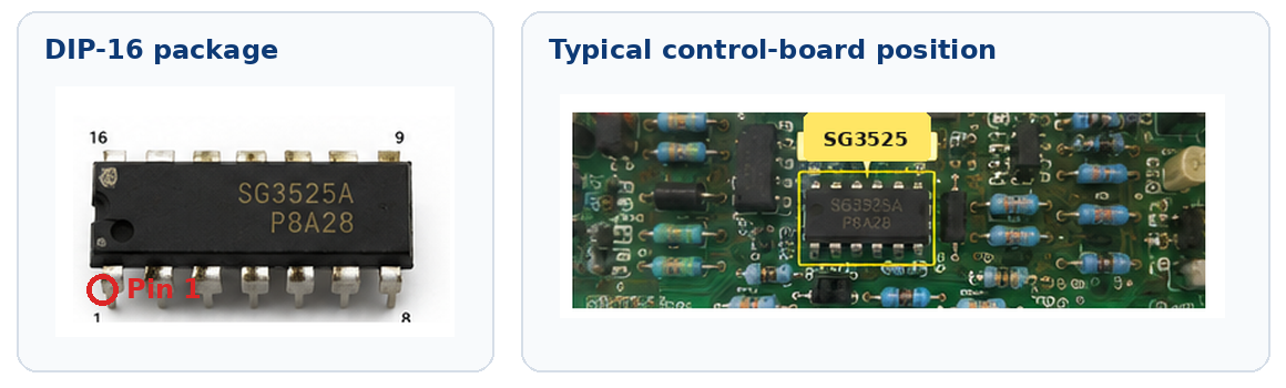
Visual identification
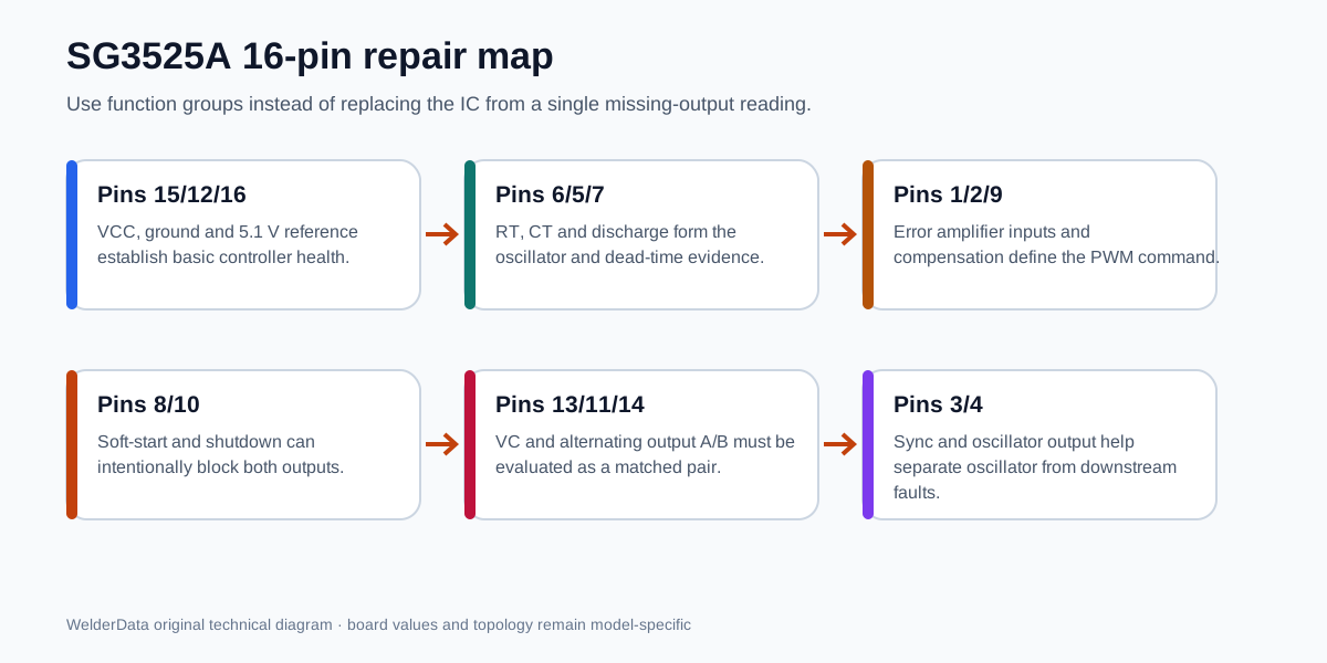
SG3525A 16-pin repair map
| Pin | Function | Repair check |
|---|---|---|
| 1 | Inverting input | Feedback and protection command. |
| 2 | Non-inverting input | Current/voltage setpoint. |
| 3 | Sync | External synchronization or noise injection. |
| 4 | Oscillator output | Clock activity. |
| 5 | CT | Timing ramp and capacitor condition. |
| 6 | RT | Timing resistor and VREF connection. |
| 7 | Discharge | Timing discharge and dead-time path. |
| 8 | Soft-start | Startup ramp; low clamp blocks duty. |
| 9 | Compensation | Error-amplifier output / PWM command. |
| 10 | Shutdown | Active trip blocks both outputs. |
| 11 | Output A | First alternating drive output. |
| 12 | Ground | Control-ground reference. |
| 13 | VC | Collector supply for output transistors. |
| 14 | Output B | Second alternating drive output. |
| 15 | VCC | Controller supply. |
| 16 | VREF | Nominal 5.1 V reference. |
Oscillator and timing faults
| Evidence | Check |
|---|---|
| VREF present, no CT ramp | CT short/leakage, RT open, pin 7 discharge path, pin 3 sync loading, damaged timing traces. |
| Frequency unstable | CT leakage, RT drift, noisy VREF, poor ground, external sync interference. |
| Pulse width abnormal on both outputs | Dead-time network, soft-start, compensation and feedback command. |
Device reference: VCC 8 V to 35 V; oscillator range 100 Hz to 400 kHz. The actual welder frequency is board-specific.
Control, soft-start and shutdown
| Node | Fault indication | Next trace |
|---|---|---|
| Pin 8 soft-start stays low | Outputs remain blocked or at minimum duty. | Soft-start capacitor, discharge transistor and protection pull-down. |
| Pin 10 shutdown active | Both outputs disabled. | Current transformer, shunt amplifier, thermal input and protection latch. |
| Pin 9 compensation forced low | PWM command suppressed. | Error amplifier, optocoupler, current/voltage command and external clamp. |
| Pins 1/2 pinned at a limit | Feedback or command fault. | Reference divider, potentiometer, current feedback and connector signals. |
Output A/B and downstream driver
| Observation | Likely area | Action |
|---|---|---|
| Both outputs missing; timing and control valid | VC supply or IC output stage. | Verify pin 13 VC, local capacitor and output loading. |
| Only A or B missing | Loaded output, damaged output stage, buffer transistor or open trace. | Compare pins 11/14 and isolate downstream load where safe. |
| A/B present at IC, absent at driver transformer | Buffer stage or coupling network. | Check transistors, resistors, coupling capacitors and transformer primary. |
| Driver-transformer secondary unequal | Transformer branch, rectifier/clamp or gate network. | Compare both branches before installing power devices. |
No-PWM workflow
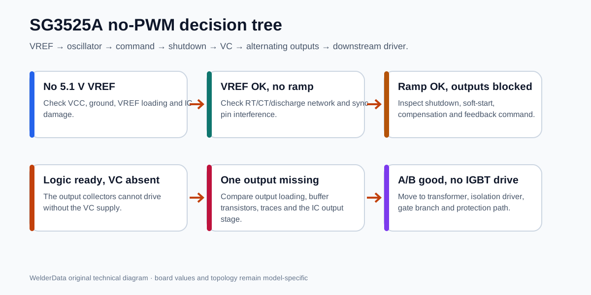
- Prove VCC and control ground.
- Prove the 5.1 V reference.
- Prove RT/CT timing activity.
- Prove soft-start and shutdown are released.
- Prove compensation and feedback permit duty.
- Prove VC is present.
- Compare output A and output B.
- If both outputs are correct, move downstream to buffer, transformer, isolation and gate branches.
Stop conditions before power-stage testing
- Do not install or energize IGBTs if output A/B waveforms are missing, unequal or overlapping.
- Do not continue powered testing with a shorted gate branch, buffer transistor or driver-transformer winding.
- Do not reference the oscilloscope ground clip to the wrong primary-side node.
- After driver repair, use current-limited staged power-up before full bus voltage and load.
Related repair map
Follow the evidence path from symptom to measurement, circuit and repair case.